
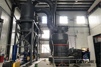
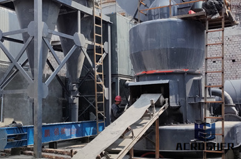
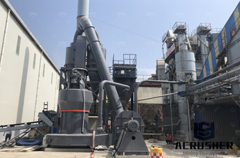
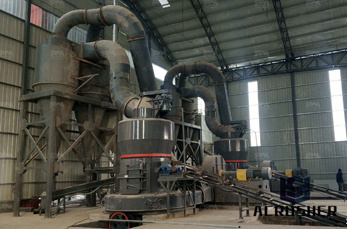
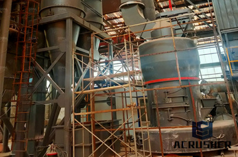
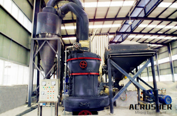
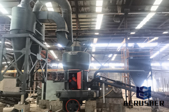
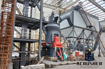
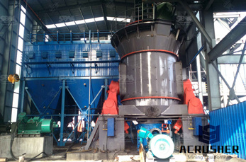
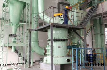
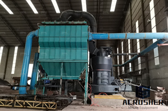
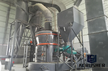
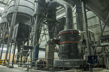
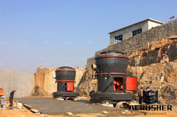
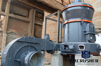
grinding process of silicon manufacturer Grasping strong production capability, advanced research strength and excellent service, Shanghai grinding process of silicon supplier create the value and bring values to all of customers.
 WhatsApp)
Dec 15, 2000· Silicon carbide is an abrasive used for grinding gray iron, chilled iron, brass, soft bronze and aluminum, as well as stone, rubber and other nonferrous materials. Ceramic aluminum oxide is the newest major development in abrasives. This is a highpurity grain manufactured in a gel sintering process.
removal thickness. An abrasive grinding wheel (typically 320500 grit) was used to rapidly remove material but it is also to greatly damage the backside surface of the silicon layer [7,8]. The second process is followed by the fine grinding process. It is used to accurately grind the wafer to the required thickness, removes most of the
Fine grinding of silicon wafers: designed experiments. on the effects of grinding wheels, process parameters and grinding coolant. As a followup, this paper reports a designed experimental study on fi ne grinding of silicon wafers. Threefactor twolevel full factorial design is used in this study.
Back grinding is a process that removes silicon from the back surface of a wafer. Silicon Valley Microelectronics provides grinding on our own substrates or on customer supplied wafers. We process bare and device patterned wafers with high yield and offer wafer thinning to customer specifications. SVM Wafer Back Grinding Capabilities:
Oct 22, 2019· The Process. The process of thinning wafers involves using a mechanical grinding wheel, chemical slurry, and IR equipment to help you measure the thickness. A classic grinding process would involve three stages: coarse grinding, fine grinding, and polishing. For example, you want to grind a silicon wafer from 725 micrometers to 50 micrometers.
During the stock removal process, a haze forms on the surface of the wafer, so an extra polishing step gives the wafer a mirror finish. After polishing, the silicon wafers proceed to a final cleaning stage that uses a long series of clean baths. This process removes surface particles, trace metals, and residues.
Our silicon wafer manufacturing process can be divided into two stages, namely, pulling single crystal ingots and slicing and polishing the silicon wafers. PolyCrystaline Silicon (Nuggets) ... Various types of grinding stones are used to shape wafer edge to meet Costomers'' unique edge shape.
Back grinding is a process that removes silicon from the back surface of a wafer. Silicon Valley Microelectronics provides grinding on our own substrates or on customer supplied wafers. We process bare and device patterned wafers with high yield and offer wafer thinning to customer specifications. SVM Wafer Back Grinding Capabilities:
side grinding of silicon wafers: a review and analysis of experimental investigations," Machining Science and Technology, Vol. 13, No. 3, pp. 285316. Abstract . Simultaneous double side grinding (SDSG) has become an important flattening process for manufacturing of 300 mm silicon wafers. However, the literature contains only a small number of
circuits is grinding process. Grinding is done to reduce the thickness and improve the surface quality of the wafer at a high throughput. Hence, its use in wafer manufacturing is increasing. Grinding is finding some newer applications in the manufacturing process such as partially replacing lapping and polishing operations.
This review paper discusses historical perspectives on grinding of silicon wafers, impacts of wafer size progression on applications of grinding in silicon wafer manufacturing, and interrelationships between grinding and two other silicon machining processes (slicing and polishing). It .
fine grinding stage provides an improved wafer thickness tolerance of mm at a slower removal rate of 20 mm/ min. In applications in which an optically smooth silicon surface is required, an additional polishing step is necessary. The most common use of the silicon grinding process is for the removal of a portion of the active wafer in the
Silicon Carbide (SiC) is a synthetic mineral most commonly produced in electrical resistance furnaces, by the Acheson process, named after the American Acheson who invented it in 1891.
Subsurface damage (SSD) induced by silicon wafer grinding process is an unavoidable problem in semiconductor manufacturing. Although experimental attempts have been made on investigation of the influential factors on the SSD depth, however, few theoretical studies have been conducted to obtain SSD depth through grinding parameters.
This review paper discusses historical perspectives on grinding of silicon wafers, impacts of wafer size progression on applications of grinding in silicon wafer manufacturing, and interrelationships between grinding and two other silicon machining processes (slicing and polishing). It is organized into six sections.
development of fine grinding of silicon wafers, a large amount of research work is needed. As the first of a series of papers dealing with fine grinding of silicon wafers, this paper reports and discusses some experimental work on the effects of grinding wheels, process parameters and grinding coolant.
Learn how to improve the quality and speed of your metallographic grinding and polishing – from selecting the best method to choosing the right consumables – with expertise, tips and insight from Struers, the world''s leading materialographic and metallographic experts.
Silicon carbide (SiC) is a compound of silicon and carbon with a chemical formula of SiC. The simplest manufacturing process for producing silicon carbide is to combine silica sand and carbon in an Acheson graphite electric resistance furnace at a high temperature, between 1600°C (2910°F) and 2500°C (4530°F).
Dec 23, 2018· This process is known as Dressing of grinding wheel and the whole process takes 15 to 20 minutes to operate. The life of the grinding wheel is described as the time period between two successive dressings. Grinding operation is one of the machining processes which consume the highest specific cutting energy with very less material removal rate.
on the effects of grinding wheels, process parameters and grinding coolant. As a followup, this paper reports a designed experimental study on fi ne grinding of silicon wafers. Threefactor twolevel full factorial design is used in this study. The objective is to reveal the main effects as well as the interaction effects of three process
Norton Abrasives St. Gobain 37C () Grinding Wheel Dressing Stick, Medium Grit Silicon Carbide Abrasive for Cleaning, Opening and Reshaping Grinding .
study the effect of grinding along crystallographic directions on the surface finish of singlecrystal silicon are reported with promising results. LITERATURE REVIEW Typical processes in the manufacturing of siliconbased devices are as follows. A seed crystal of silicon is placed on the end of a rod and dipped into a vat of molten silicon.
Wafer backgrinding is a semiconductor device fabrication step during which wafer thickness is reduced to allow stacking and highdensity packaging of integrated circuits (IC).. ICs are produced on semiconductor wafers that undergo a multitude of processing steps. The silicon wafers predominantly used today have diameters of 200 and 300 mm. They are roughly 750 μm thick .
Silicon carbide: Silicon carbide grinding wheels are made by mixing pure white quartz, petroleum coke and small amounts of sawdust and salt, and then by firing the mixture in an electric furnace. The process is called synthesizing the coke and sand.
WhatsApp)