
japan silicon edge grinding equipment manufacturer Grasping strong production capability, advanced research strength and excellent service, Shanghai japan silicon edge grinding equipment supplier create the value and bring values to all of customers.
 WhatsApp)
TOP. Introducing the Edge Grinder series that brings NCcontrolled grinding to the chamfering process on silicon and other wafers for the first time in the world. Besides the WBM series, in wide use and still regarded as the industry standard, we will be releasing the new highprecision CVP series of chamfering systems. ...
offers 61,392 japanese silicone products. About 1% of these are other metals metal products, 1% are adhesives sealants, and 1% are seals. A wide variety of japanese silicone options are available to you, such as filling machine, fashion.
Tips on Fine Grinding Stainless Steel Choosing the right equipment and consumables to grind a fine finish on stainless steel can get the job done faster with less operator fatigue. Here are nine ways to create a smooth surface in some typical finishing applications.
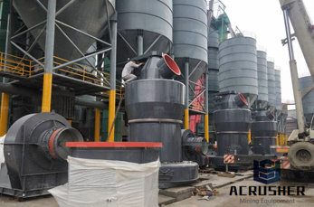
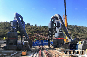
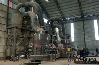
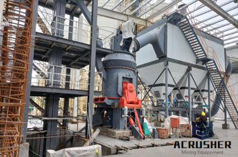
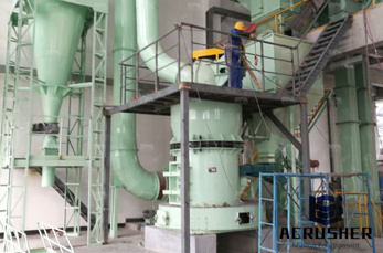
It is the page for our semiconductor manufacturing equipment. It introduces such as wafer manufacturing system, SMP, Wafer probing machine, Polish grinder, Wafer dicing machine, Highrigidity grinder and Blade for precision cutting.
surface grinding in silicon wafer manufacturing wire sawn wafer grinding, but will also briefly cover another application etched wafer grinding. Following this introduction section is a description of the surface grinding process. After that, the applications to wire
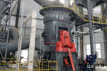
We manufacture premiere CMP, grinding and substrate manufacturing equipment for use in the production of semiconductor devices. Every piece of equipment from Revasum is designed with the customer in mind; as a result, each one meets or exceeds our customer''s performance targets.
japan silicon edge grinding equipment; japan silicon edge grinding equipment. Grinding Machines Products | NTC Ltd. Indeed, NTC grinding machines used to be a subject of adoration in both the domestic and overseas markets. The mythology in these words has further evolved. Cylindrical grinding machines .
Newlydeveloped grinding unit enhances the rotative precision of the spindle, and improves the surface roughness. The noncontact measuring method achieves the stable alignment. Performs the noncontact measuring of the preprocessed wafer thickness at multiple points, the diameter and notch depth of the postprocessed wafer.
Wafer Edge Grinders. Since introducing the world''s first Numeric Controlled Edge Grinder over 30 years ago, Daitron has continued to make improvements in quality and yield to the processing of Silicon and other semiconductive materials. The latest VTwin contouring technology utilizes the 2 axis vertical grinding process. This system assures ...
Grinders can thin silicon wafers, compound semiconductors, and many other types of materials with a high degree of accuracy. Processing for applications which use the DBG system or DAF (Die attach film) is also possible by incorporating a polisher and wafer mounter with the grinder into an inline system*.
TAIKO is a DISCO developed wafer back grinding method. By enabling an outer support ring to the wafer (the TAIKO ring, Japanese for drum), back grinding is performed on the inner circular area of the wafer, while leaving an edge of a few millimeters unprocessed. .

Jan 25, 2016· Ever wonder how silicon wafers get so thin? What are the processes involved in polishing a coarse wafer into a usable and highgrade silicon wafer? Find out in the video! #silicon #siliconwafer.
japan silicon edge grinding equipment; japan silicon edge grinding equipment. Grinding Machines Products | NTC Ltd. Indeed, NTC grinding machines used to be a subject of adoration in both the domestic and overseas markets. The mythology in these words has further evolved. Cylindrical grinding .
: Over Molding Process Development for a Stacked WLCSP (4/10) MC3 mold materials with the different package structures. The material basic properties and technique are shown in Table 2. This evaluation was done with grinding and larger 2nd chip size. The exposed chip tends to show lower warpage and the 2nd chip reduces wafer warpage.
Edge Grinder. Edge Grinder is equipment to grind edge of all kinds of substrate materials for a specified profile. Our wide range of Edge Grinder lineup can support substrates of any material kind, such as silicon, metal, SiC, sapphire and oxide substrates, featuring easy operation and .
The slanted or rounded edge between the bottom of a wafer and the side of a wafer is the bevel region. Beveling is achieved by edge grinding, or pressing the edge of a grooved grinding wheel against the wafer as it rotates. Beveling wafers can help to prevent chipping and can have an impact on the function of the semiconductor when it is finished.
As the leader in Kiru Kezuru Migaku technologies, DISCO pursues excellence in solutions support with decades of experience, a full range of processing equipment, and several thousand different grinding wheels, polishing wheels, and blades.

A professional tool grinding center should also continuously study the experience in order to make the tool better and more professional. Here are 6 problems that cannot be ignored from the perspective of the tool itself, grinding equipment, testing equipment, grinding standards, and grinding mechanics. Tool and cutter material
Polishing Grinding Manufacturers Wafer Production Equipment Companies involved in Polishing Grinding machine production, a key piece of equipment for the production of solar wafers. 21 Polishing Grinding equipment manufacturers are listed below.
Edge chipping of silicon wafers in diamond grinding. ... an optical microscope (MX40, Olympus, Japan) was utilized to observe edge chipping. The optical image of edge chipping was then imported into the AutoCAD software for chipping edgeprofile approximation and chipping area calculations. ... In grinding a silicon wafer by a diamond wheel ...
Semiconductor Wafer Edge Analysis/6 Figure 3 shows an example of an edge measurement of a thin bonded wafer. This demonstrates defects leading up to and within the transition region of a rounded wafer edge. The upper plot shows the roughness calculated with a high pass filter (cutoff filter) of 250 µm over a distance of 6,000 µm.
SEMI Edge Profile WG Abstract A survey was designed and distributed to device manufacturers in Japan and the US in order to solicit their views on the need for a more precise characterization of the silicon wafer edge profile. It is believed that the current edge profile template
Learn how to improve the quality and speed of your metallographic grinding and polishing – from selecting the best method to choosing the right consumables – with expertise, tips and insight from Struers, the world''s leading materialographic and metallographic experts.

Edge Polisher. The EPD is a system which improves the Wafer Edge by polishing patterned wafers. The EPD removes foreign and unwanted substances from the edge bevel at critical process nodes. SpeedFam is the pioneer of Edge Polishers for the production of prime wafers. We make use of this system with astonishing results on 300mm, 200mm, and ...
WhatsApp)